Friday, November 4, 2022

Xilinx FTDI without a Digilent license

Xilinx FTDI without a Digilent license. Starting from 2022.2 (or earlier?) Vivado distribution includes an FTDI programming utility that makes the FTx232 devices visible in the Vivado hardware manager. So no need anymore for the secret and invisible Digilent license string! UPDATE the invisible license is still needed, it is silently written...

https://docs.xilinx.com/r/en-US/ug908-vivado-programming-debugging/Programming-FTDI-Devices-for-Vivado-Hardware-Manager-Support 

This is nice that we do no longer need to use the licensed FTDI tool to write into the hidden User EEPROM for Xilinx tools to recognize the programmer dongle. Well, the hidden EEPROM is still used and needed, so if we use FT_PROG to write the FT2232 EEPROM, the hidden license will disappear and the programmer will not be recognized anymore.

Interestingly the provided schematic does not provide support for the Zynq SRST pin :(

Interestingly this Xilinx forum post seems to describe some more used pins:


Thursday, October 27, 2022

Configuration of FPGA with MCU.

 How to configure Xilinx FPGA with MCU using JTAG? This is actually pretty simple, pseudocode:

send_header();

send_raw_bistream(bitstream);

send footer();

The functions send_header and send_footer do some TDI/TMS toggling, send_raw_bistream sends raw bitstream data from the bitstream to FPGA TDI pin (note bit order in the bitstream!).

How to implement send_header/send_footer? The easiest and smallest footprint for the MCU is to implement 2 bit playback function, so the pseudocode would look like this:

send_tdi_tms_bits(header_2bit_file);

send_raw_bistream(bitstream);

send_tdi_tms_bits(footer_2bit_file);

How to get the 2 bit sequences for the header/footer? OK, this is one known working and relatively simple approach:

1) You generate with Xilinx Vivado an SVF file for your target device. If you look at the generated SVF you can quickly see three sections there, there is a header, then raw content, then a footer. Look at header/footer only, you do not want to convert to 2bits the raw data.

2) cut out the header and footer with some text editor

3) remove the ID code check lines from the header, you do not need that! And your MCU playback would be WRITE only with no readback or verify functions.

4) get SVF player code from say maybe here: https://github.com/xaxaxa-dev/svfplayer it looks like useable but I have not compiled this code myself

5) modify the SVF player to emit 2 lower bits of each processed byte, this is an easy exercise for anyone with moderate C experience.

6) play header and footer SVF files with your SVF_to_2bitsfile.exe you created in the previous step.

7) implement for your embedded MCU function send_tdi_tms_bits() and send_raw_bistream(). Use the pseudo code from above on your MCU to configure the FPGA.

OK, there is a little bit of tweaking required, you possible need to insert a delay during header playback, and the line RUNTEST 10000 TCK; should possible also be implemented as direct code with your MCU sending 10,000 TCK cycles without change on TDI/TMS.

OK, the idea should be clear. Happy bit toggling!

How to do it on Rasperry Pi PICO? First of all we need wiring, to save time on the documentation we can take the Pico pin mapping from here: https://github.com/phdussud/pico-dirtyJtag/ Already saved some minutes of work :)

Now we need the function send_tdi_tms_bits as this function is rather short compared to the main junk bitstream pushing we can use machine.Pin class it will be slow but it does not matter. We assume that the 2bit file is generated with the svfplayer with TMS being bit 0 and TDI being bit 1 in the saved file.

from machine import Pin

tms = Pin(19, Pin.OUT)   # TMS: create output pin on GPIO19
tms.on()                 # set TMS to "on" (high) level
tdi = Pin(16, Pin.OUT)
tdi.on()
tck = Pin(18, Pin.OUT)
tck.off()
The above creates pins for TCK, TDI, and TMS, as we are WRITE only interface we do not need to assign TDO to anything, we will not use TDO at all.

Now my python skills are not enough :( but let's give some hints how to proceed:

def send_tdi_tms_bits(byte_with_2bits_in_it)
    tms.value(byte_with_2bits_in_it & 1)
    tdi.value(byte_with_2bits_in_it >>1 & 1)
    tck.on()
    tck.off()

ready :) OK I mixed C and python programming(or did I?). This function needs to be called with the bytes our svf_to_bits converter wrote for the header and footer.

Now, what's next? We need to send the bitstream too right? OK, we can do it using the machine.Pin functions but it would be really slow. OK, for the proof of concept it does not matter.

Later we should optimize the bitstream push using the Pico PIO peripheral, some links:


This is now beyond my current python skills, so it is left to the reader to implement the bit sending with PIO.


Thursday, June 30, 2022

Lattice AVANT is coming

There is not much info published yet, but if you google "Lattice Avant" you get some stories about it. What is known: released date H2 2022, so at the end of the year we should hear more about this product. FPGA core size at least 300,000 Logic Cells. That's about all that is known without NDA. Excited, only a few more months to wait.

Avant official release will be 5 December 2022! So then we can all talk more.


Friday, June 3, 2022

Java to FPGA

Surprise, surprise, at least two projects promise java 2 RTL (VHDL, Verilog) conversion suitable for execution on FPGA!

Java2VHDL is currently only experimental but LED blink at least works. The current work seems to support directly only Lattice Diamond tools. Here is a link to the project Java2VHDL. The LED blink and other examples are tested on this tiny board XO2000.

---

There is another Java converter, called synthesijer, with web and GitHub for project code. This project uses Xilinx evaluation boards as target hardware.


Monday, May 30, 2022

ArrowBlaster Internals


 ArrowBlaster (TEI0004) and ArrowBlaster SMD (TEI0005) are both based on FT2232H USB FIFO chip. There are no custom OS drivers involved, the standard FTDI drivers are used for both. What is downloadable from Trenz Electronic website as "driver" is actually a DLL/SO dynamic library for Windows/Linux for Quartus to recognize the programmer hardware. This DLL uses channel A (ADBUS0..3) in MPSSE mode to access the standard mapping JTAG pins connected to it. ADBUS7 is connected to RED LED (active low) and it is used as a busy indicator by the Arrow software DLL.

Quartus <> Arrow "driver" DLL <> D2XX library DLL <> FTDI USB drivers

ADBUS4 (named PROC_RST on TEI0004) is described in the documentation as "for future use" but it is highly unlikely that the Quartus DLL will ever utilize this pin. So it is free for use by the end-user applications. So at any time when the Quartus is not accessing JTAG ADBUS4 can be controlled by the user application over D2XX DLL/SO. One example of usage would be control of the JTAG Enable signal - some FPGAs (like MAX10) can use the dedicated JTAG pins in User Mode. During programming and debugging the JTAG would be enabled, and then in user mode, the end-user application would access ADBUS0..3 via D2XX say like an SPI port between the user application and the FPGA code. FTDI provides lots of examples of D2XX library use.

Arrow driver does not access channel B at all, so it is free for the end-user at all times. Channel B is free for end-user to be used as an extra UART channel to the FPGA. On TEI0005 there is one more pin BCBUS0 available to the end-user. This could be controlled over D2XX DLL easily. It is also possible to control the UART function over D2XX so in this case, the end-user could use port B UART and one GPIO pin at the same time. Another use case could be channel B as UART via VCP drivers, and channel B ADBUS4 as GPIO over D2XX at the same time (Quartus not active).

Third-party software that supports FT2232H can also use these adapters. One example application is SVF player.

FT2232H EEPROM is programmed with "Quartus License" information, if you erase or over-write it, then Quartus would no longer recognize the dongle. It is possible to convert the adapters to Microsemi programmer (TEI0004 VREF pin would not map to Microsemi pinout so custom wiring is needed in that case).

Some use cases:

Case 0:

  • Channel A - Quartus or 3rd party FT2232 JTAG software active
  • Channel B VCP UART
  • ADBUS4 not usable
  • BCBUS0 not usable

Case 1: 

  • Channel A - No JTAG software active, or custom D2XX software
  • Channel B VCP UART
  • ADBUS4 D2XX custom software GPIO1
  • BCBUS0 not usable

Case 2: 

  • Channel A - No JTAG software active, or custom D2XX software
  • Channel B D2XX UART
  • ADBUS4 D2XX custom software GPIO1
  • BCBUS0 D2XX custom software GPIO 2

Friday, May 27, 2022

Xilinx 3.3V LVDS

Sometimes we have a Xilinx 7 series FPGA board with 3.3V VCCIO (HR bank) and we need LVDS output in those banks. What to-do? Selecting LVDS for those banks will not work at all, because Xilinx 7 series IO drive circuits include a VCCIO comparator that switches the differential (except TMDS_33) outputs off if the VCCIO is above 2.65V.

Solution 1: We select LVCMOS33 and use complementary outputs in RTL code. This is a very rude approach, but it may in some rare cases be acceptable.

Solution 2: We use LVCMOS33 outputs with an external resistor divider network (3 resistors) to adjust the differential output voltage to LVDS levels.

Solution 3: We use TMDS_33 outputs with 50 ohms pull-up resistors to 1.5V. This is the best solution, but it needs external termination voltage.

Solution 4: We use TMDS_33 outputs with a 100ohm resistor divide option, one resistor from signal to ground, and one resistor from signal to 3.3V supply (4 resistors total). This should also be a somewhat acceptable solution.

Solution 5: We use external CMOS to LVDS buffer IC.

Differential inputs work at 3.3 VCCIO, only on-chip termination is not available, so you need an external 100ohm parallel termination resistor for inputs.

See also Xilinx answer record 43989


Monday, May 9, 2022

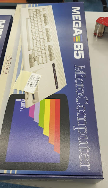
MEGA65 ready for shipping

 The first real batch of MEGA65 retro computers is ready for shipping!

Tested MEGA65 units waiting to be boxed into the real shipping boxes, with color print on the boxes.
Really colorful!
More packaging boxes inside the colorbox!
The colored box is then inserted into the outer shipping box before sending it away.


Wednesday, April 27, 2022

Lattice Propel it's easy!

Lattice is promoting its easy-to-use RISC-V design tool for some time already, but well I did not have suitable target hardware, well until now.


This is a small development board with Lattice Certus NX FPGA and CRUVI host slot and pin headers (visible in the bottom layer). Board available here: CR00103 shop.

OK, let's start the Propel ding! 

Run Propel, and select new workspace (an empty location on the hard drive). 

File New, Lattice SoC design project. Setting project name, select the device name, and select template design "Hello World Project". Done. Now let's set up the SDK project too. 

File new, Lattice C/C++ Project, finish. Build the C project. Done.

And we are done with the Propel/SDK now let's see how we can build the FPGA design. From the main menu LatticeTools, select "Open design in Propel Builder". Propel Builder launches and displays a block diagram of the SoC system.


Checking that SDK compiled memory image is assigned properly:

Now we have really done with the Builder.

Click on Generate and then another click to launch Radiant for back-end work. In Radiant, we need to add IO constraints. This is tricky we need to set the PDC filename to match the name of the project or it would not be found later.
Done, empty constraint file exists at the proper location. Now we need to set the constraints to match the board IO. I have them ready so I just copy them from another project. 

ldc_set_location -site {A8} [get_ports {led_o[0]}]
ldc_set_location -site {B8} [get_ports {led_o[1]}]
ldc_set_location -site {B2} [get_ports rstn_i]
ldc_set_location -site {C11} [get_ports rxd_i]
ldc_set_location -site {F11} [get_ports txd_o]
ldc_set_sysconfig {INITN_PORT=DISABLE}

Done.

Now we can click on "Export Files" and go grab a coffee or two while the design runs. Bad luck the design is already completed no time to bring another coffee. Does it work? Setting up UART console at 115200 baud. Starting the programmer! Done! And voila we have hello world! It worked!
We have Hello World running on Certus-NX FPGA!

Now I need to select the necessary files and create a reference design archive so others can start quickly with this board. But it's basically easy. It just works. Can it be just that simple? Well seems like, it worked first try!